Design focus: parasitic inductance
Powering a high frequency digital circuit means providing a supply with an adequately low impedance across the entire frequency range from DC up to the highest frequency present in any digital switching edges. Correctly designed power distribution is crucial to achieving reliable operation and low RF emissions.
The frequency range over which a power supply must maintain low impedance is a function of the fundamental switching speed of the device used, not simply the number of edges per second. This means good high frequency decoupling is required regardless of whether the clock is running at just a few Hz, or hundreds of MHz, or somewhere in between.
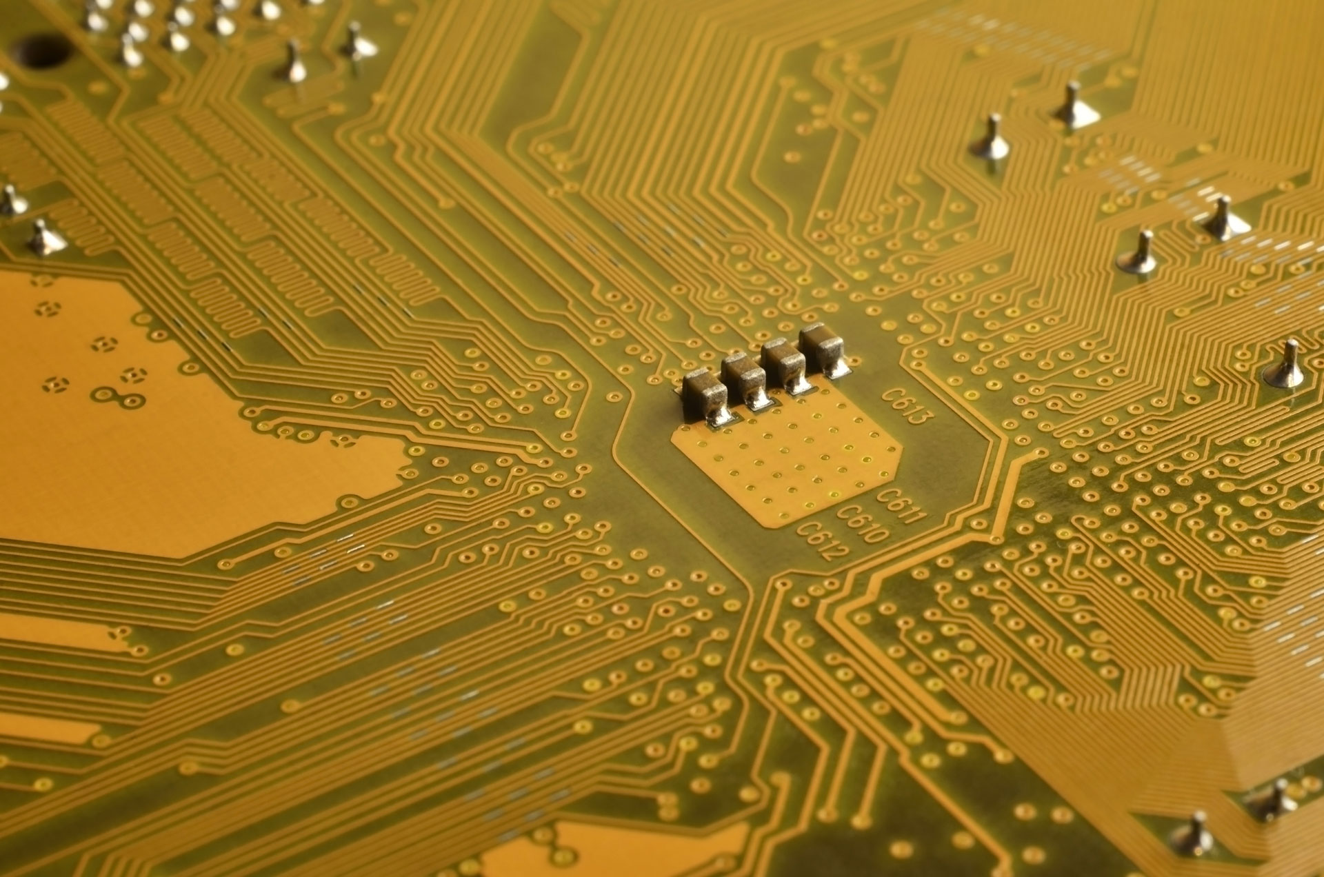
Before starting a high speed PCB layout, it’s worth taking a moment to do a few rough calculations. For a trace 0.15mm (6 mils) wide in 1 oz copper, the inductance of 1mm is ~0.6nH. This will resonate with a 100nF capacitor at 20.5 MHz, and at frequencies higher than this the impedance of the supply is dominated by this inductor, not the capacitor.
All this happens at frequencies which are much lower than the frequencies contained within digital switching edges, which is why great care must be taken in the placement and routing of decoupling caps in digital circuits. The parasitic effect of a short PCB trace may completely negate the benefit of a decoupling capacitor in a given location.
Conversely, it may also be possible to minimise the number of decoupling caps that are required in a given design by improving the layout.
– Remember that it is inductance, not resistance, that dominates the impedance between two points on the PCB.
– The lowest inductance route between any two points is through a solid, uninterrupted plane – even if this means the path length between them is greater than it would be if they were joined by a thinner trace on the same layer. The shortest physical distance may not correspond to the shortest electrical distance.
– The parasitic inductance of a ceramic capacitor depends on its physical size. For two capacitors of equal case size (eg. 0402) but different values, the one with the higher value will have a lower impedance at most frequencies than the one with the lower value, making it the better choice for decoupling.
– A single capacitor joined into its power plane with two traces and vias at each end may be just as effective as two separate capacitors routed with one trace and via each. That same capacitor connected using planes on the component side of the PCB, and stitched into the buried power and ground planes using multiple vias, will be more effective still.
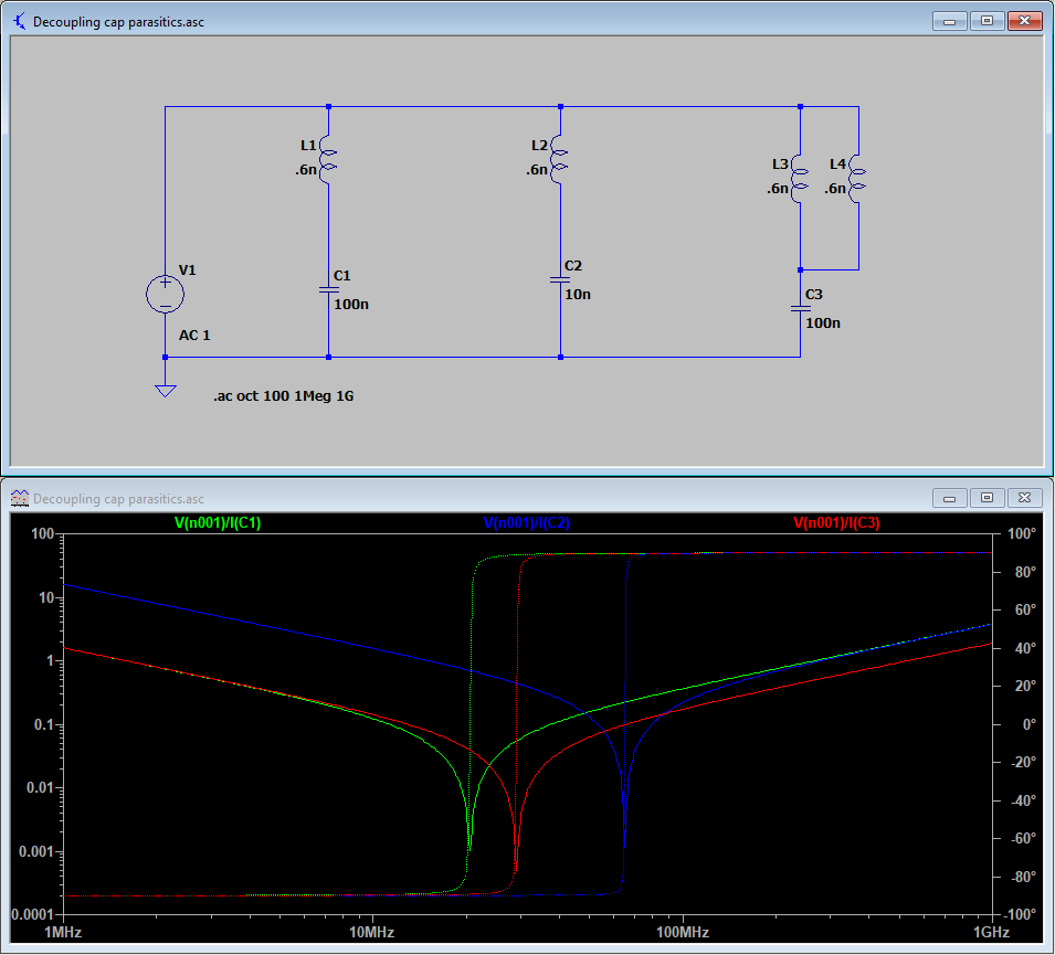
A SPICE simulation clearly shows the difference:
– the green trace represents the impedance of C1, value 100n, with 1mm of trace attached. Resonance occurs at 20.5 MHz as expected, above which the inductance becomes dominant.
– the blue trace represents C2, which is 10n but otherwise identical. Although resonance occurs at a higher frequency (65M), the absolute impedance of C1 (and its ESL) is still significantly lower all the way up to 48M, and there’s negligible difference from 100M upwards where both become dominated by their ESL.
– the red trace shows a single 100n capacitor but connected by two traces in parallel rather than just one. Its impedance is lower than either of the other two across the entire frequency range apart from a very narrow window where the 10n cap resonates. In particular, it maintains a significantly lower impedance at high frequencies.
Simple changes to a board layout can improve its high frequency performance enormously, and a clear understanding of how the layout will affect the performance of the design is crucial to producing boards which are reliable and which can pass EMC testing.
Do you have a new digital design project in mind?
Or a board which is failing emissions testing?
CEL has years of experience in high speed board design and layout, signal integrity and EMC.
Contact us today to see how we can help.
 01252 511577