How are high speed digital signals terminated on a PCB?
This article explains why termination is needed in a high speed digital design, and why different types of termination are used.
What is a transmission line?
At high speeds the traces on a PCB can no longer be regarded as simple wires that cause two points on the board to always be at exactly the same potential. A PCB trace has series inductance and resistance, and distributed along its length it has capacitance to ground.
These parasitic elements are impossible to eliminate, but their values can be determined from the geometry of the trace and the stack-up of the PCB. For simulation purposes the trace can be modelled as a string of discrete inductors and capacitors; the pure dc resistance is usually negligible in high speed applications and can be ignored.
A not-at-all-obvious mathematical result is that a free end of a long PCB trace, routed on a layer above a GND plane, behaves like a resistor to GND. This behaviour persists for as long as it takes a propagating wave to travel the entire length of the trace and bounce back toward the transmitter; if the trace were infinitely long, the round trip time would also be infinitely long, and the trace would look just like a resistor to GND indefinitely.
The value of this “resistor” is called the characteristic impedance of the trace. The amount of time for which the trace looks like a resistor depends on the round-trip delay for a wave propagating along it, which in turn depends on its geometry, materials and length.
A PCB trace (or other conductor) which is long enough that this behaviour must be taken into account is referred to as a transmission line.
Why does signal integrity matter?
The input of a digital device has a maximum voltage that is guaranteed to represent a logic ‘0’, a minimum that is logic ‘1’, and a region in between through which the signal must transition monotonically if the device is to function reliably. This is of particular importance on clock inputs, where any reversal of direction within the transition region can cause the receiver to switch multiple times, resulting in data corruption.
Let’s now consider what happens when a high speed edge is generated at the output of a digital device, and switches from a logic 0 (0V) to 1 (3.3V). For the purposes of this example, the edge has a rise time of 200ps and switches at a rate of 10 MHz.
The first thing to note is that the 10 MHz switching rate is irrelevant. The phenomena which govern signal integrity on a high speed signal relate to the edge speed, not the number of edges/sec, so slowing down the clock makes absolutely no difference to whether or not a given layout will work properly.
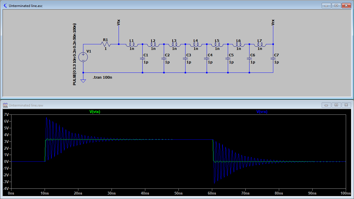
In the first example, the PCB trace is modelled as a string of discrete L-C blocks, each consisting of 1nH in series and 1pF to GND. As a rough rule-of-thumb, 1mm of trace equates to 1nH of inductance, so this trace is not in fact particularly “long” in absolute terms. The characteristic impedance of this particular trace is about 32 Ohms, which is within the normal range for a mass produced multilayer board using conventional geometry. The transmitter is modelled as an ideal voltage source with 1 Ohm output resistance and a rise time of 200ps.
The signal at the transmitter switches cleanly from 0 to 3.3V in the expected 200ps and looks fine, but the signal at the receiver is very different. It peaks at over 6V and oscillates many times before eventually decaying away and setting at the expected logic ‘high’ level. The falling edge behaves the same way and dips below -3V before settling to GND potential. Not only does the signal contain multiple switching edges that can corrupt data and cause clocked circuits to misbehave, but the voltage swings can easily exceed the absolute maximum ratings for the receiver and damage it.
To understand why this occurs, we can look at the components in our trace model at each end of the line. When the output of the driver goes high, C1 is initially discharged and L1 sees the full logic supply voltage across it. This causes the current through L1 to ramp up, charging C1, and so L2 starts to see a voltage, and so on. The voltage wave propagates from transmitter to receiver, charging each capacitor in turn, until the wave reaches the final elements in the chain. This doesn’t happen instantaneously; it takes time, which depends on the inductance and capacitance per unit length of trace.
Since the receiver is high impedance, any current through the last inductor has nowhere to go other than the final capacitor element (which will also include the parasitic capacitance of the receiver, and possibly your scope probe if you have one connected). This current charges the capacitor, causing the voltage across it to increase.
The increase continues until the current through the final inductor reaches zero. This occurs when the voltage at the receiver Vrx equals 2x the initial height of the edge at the transmitter Vtx, and results in the wave propagating back along the trace in the opposite direction, back towards the transmitter.
This doubling of voltage and reversal in direction is characteristic behaviour of an unterminated transmission line.
Image shows Unterminated line

When the wave arrives back at the transmitter it must meet another boundary condition, namely that the voltage at the output of the transmitter is fixed, but the transmitter can sink or source current in order to maintain this state. The transmitter must now sink current in order to maintain a constant output voltage, and the result is that the wave once again reverses direction and propagates back towards the receiver.
Because neither an inductor nor a capacitor can dissipate energy, the energy has nowhere to go except to transit up and down the trace repeatedly, resulting in the rapid oscillation we see. It eventually decays away because of the 1 Ohm output resistance in series with the transmitter; without this, oscillation continues indefinitely.
Clearly this is not usable.
How does series termination improve signal quality?
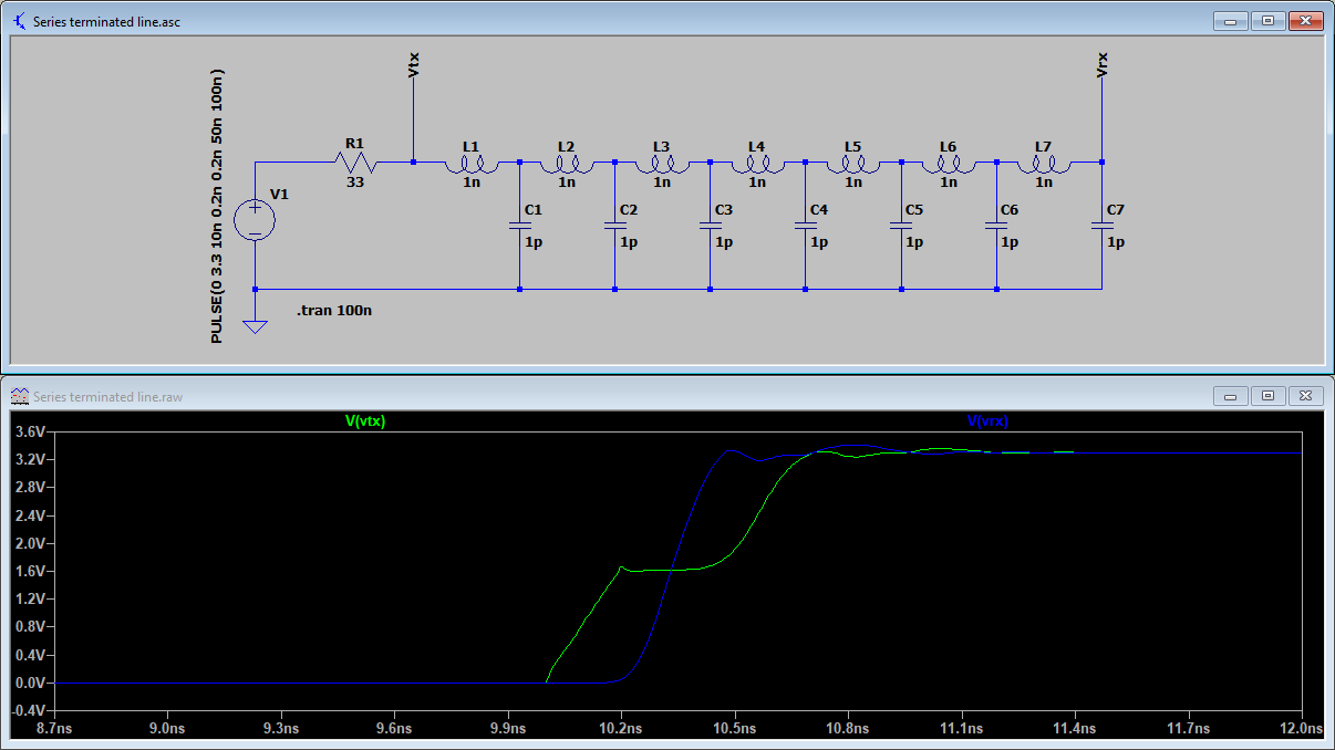
Now let’s consider what happens if we put a resistor, with a value equal to the characteristic impedance of the trace, in series with it. The resistor is physically located right next to the transmitter, and adds to the internal resistance of the driver. This topology is referred to as ‘series termination’.
Image shows Series terminated line

The signal at the receiver is now clean and square – but why?
The signal at the transmitter itself is the same, but recall that the PCB trace looks like a resistor to GND until the wave has completed a full round-trip. This resistor forms a potential divider with our series terminator, resulting in an output voltage at the start of the trace which is exactly half of the logic ‘1’ level. As before, this wave propagates along the trace toward the receiver, whereupon it doubles in amplitude and reverses direction.
Now, though, rather than presenting a problem, this doubling of amplitude is exactly what’s needed to make the signal reach a valid logic ‘1’ level. The voltage at the receiver switches monotonically from logic ‘0’ to ‘1’ just as required.
The reflected wave travels back up the trace to the transmitter, but now instead of meeting an (ac) short to GND, it sees an impedance equal to the characteristic impedance of the trace. In terms of its electrical characteristics, this resistor looks to the wave just like an infinitely long extension of the transmission line, so there is no reflection; instead, the energy in the wave is dissipated as heat in the resistor, and the current in the trace falls to zero. With zero current flowing in the potential divider, no voltage is dropped, and so the voltage on both sides of the termination resistor now equals the full logic ‘1’ level and the system is stable.
This termination scheme is popular but is not without problems. A clean, monotonic edge is seen at the receiver, but not at the transmitter, nor at any other point along the length of the trace. Instead there’s a period of time for which the voltage sits at half the logic ‘1’ level, which is right in the middle of the transition region for most digital inputs, and likely to cause problems. Therefore, series termination is generally OK for point-to-point routing (one driver / one receiver), but is not suitable for cases where a single output must drive multiple inputs located in different places on the PCB. If one output must drive multiple inputs, then each input must have its own trace and series terminating resistor.
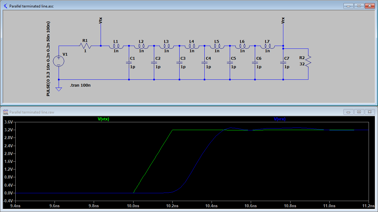
Another option is parallel termination. In this case a resistor, again equal to the characteristic impedance of the trace, is connected between trace and GND at the receiver.
There is no dividing down of the output voltage at the driver, so a wave with an amplitude equal to the full voltage swing of the driver travels along the transmission line.
When the wave arrives at the receiver it is immediately absorbed by the terminating resistor, which looks to the wave like an infinitely long extension of the trace. No reflection occurs, so the system reaches steady state after a single transit time. Every point on the trace transitions cleanly from logic ‘0’ to ‘1’ subject only to a pure propagation delay, and so high impedance receivers can be connected at any point or points along the trace.
This makes parallel termination useful for distributing clocks and other common signals to which multiple devices must be connected, but there’s an important caveat – the dc current is not zero. In this example, using 3.3V logic and a 32 Ohm trace, the driver must continually source 100mA, and the terminating resistor must dissipate 320mW of heat. Often this is not acceptable for power and thermal management reasons.
Parallel termination can also be used in multi-master interfaces, by putting a terminating resistor to GND at both ends of a long trace. Multiple drivers and receivers can be located along its length, and good signal quality is seen at every point on the trace. Terminating both ends of the transmission line does, of course, doubles the wasted current, but is still useful in applications such as long backplanes which may be driven from any one of a number of plug-in cards.
As well as being used on PCBs, parallel termination is also used in interfaces such as the automotive CAN bus.
Image shows Parallel terminated line

What other options for termination are there?
One other option, less often used, is to parallel terminate with an R-C network. A capacitor is used to block the dc current, and a resistor provides termination for ac signals as before. This can be beneficial, but has problems of its own; a real capacitor has ESL and can introduce frequency dependent issues that are hard to predict or probe.
Another option is to terminate not to GND, but to an intermediate voltage half way between the logic ‘0’ and ‘1’ levels. This reduces the wasted current by half, and for a signal which spends 50% of its time in each state, the average power wasted in the terminating resistor is also halved. One common interface which uses this mid-point termination voltage is DDR2.
Conclusions
– The need to treat a PCB trace as a transmission line, and terminate it correctly, depends on how long it is and how fast the driver switches between ‘0’ and ‘1’.
– A poorly terminated design which is experiencing errors due to signal integrity can NOT be made to work by slowing the clock down.
– Successfully designing a high speed digital system requires good knowledge of the underlying physics.
Need Help ? Contact Us
Electronics Product Design
Whether you have a detailed specification or just a bright idea, we can help you turn it into a production ready design, backed up by all the CAD data and software, plus the support you need for as long as you need it.
Fix & Improve
Do you have an existing design with a problem, or which doesn’t quite do what you need it to? CEL can help make it better.
The Process
We’re keen on communication. Let us take the time to really understand what you need, and explain how we can help.
Specialist Areas
Need something a little out of the ordinary? We may well have been there before.


 01252 511577