All Posts By

Cawte Engineering

Dealing with the supply crisis in electronics

Dealing with the supply crisis in electronics

Photo by Jasmin Sessler on Unsplash

If you’re in the business of making and selling electronic products, you can’t help but have been dismayed by the lack of stock, extended lead times and price hikes which have plagued the supply chain for components over the last year or more.

It doesn’t help that manufacturers are, in many cases, not engaging well with SMBs whose businesses depend on the parts they’ve designed in. Look at the home page for any major IC manufacturer; rather than saying ‘click here for an up to date delivery schedule and to place your order’, it’s still the usual marketing fluff, as though nothing was wrong.

But something is very, very wrong.

How did we get here?

Various factors have contributed to the shortages:

– Misjudgment of demand by IC manufacturers during Covid lockdown. Instead of sales of IT equipment slowing down as predicted, people instead went out and bought new laptops, cameras and other equipment so they could work from home – a trend which still continues today. Inventory levels throughout the supply chain had been allowed to reduce, only to see a sudden spike in demand.

– Closing of factories in the Far East. As part of their national strategy to reduce the spread of Covid, manufacturing facilities have been closed for weeks at a time, with predictable consequences.

– Hoarding and reselling by speculators. As soon as components arrive with distributors and become available for sale, grey market resellers have been buying them up in bulk, only to immediately try and resell them at an enormous mark-up. Genuine customers, meanwhile, have often had little choice but to pay well over the odds for goods of unknown provenance, or to somehow do without.

– Pestilence, war, famine, and years of chronic [insert practice here] by [insert entity here], depending on who you talk to and their political leanings. Everybody has their own strongly held opinion as to why the market is in quite the state it’s in, most are probably right to some degree or other, and at the end of the day, for us as engineers and manufacturers who just want to stay in business and make a living, it doesn’t really matter anyway.

– Stockpiling by manufacturers. A necessary evil that we’ll get on to…

What can we do?

1) Contact your suppliers

Your first calls should be to the suppliers from whom you purchase components. Just because components aren’t making it to the shelves as free stock doesn’t mean there aren’t any deliveries taking place; components are still being manufactured, but most are being allocated to existing orders since there aren’t enough to go round and clear the backlog at the same time.

If you don’t have an order in place with your distributor (or manufacturer), then you probably won’t be seeing the critical component you need any time soon. If you do, though, then there’s a fair chance that you will – provided you’re prepared to be patient, and possibly pay upfront.

Do be aware, though: delivery dates can and do vary. You may be lucky and get a surprise package from a courier that wasn’t due until next Easter, or you may receive a weirdly unapologetic email telling you your new delivery date is 6 months later than you were promised, with no explanation as to why.

(Spoiler: it’s because the wafer containing your chips was sold to a bigger company with a much larger annual spend on ICs than you have).

2) Buy what you can, when you can

The decision on how many to buy should be straightforward to calculate. Work out the cost of any excess parts you might never use, and compare this with the cost to your business of not being able to manufacture your product because a part is missing.

Buy a number of complete kits – not an excess of any one particular device unless it’s one you use in multiple products – plus spares to cover yield and wastage.

Assume that, when a part becomes available to buy, it might not come up again any time soon.

Bear in mind that it’s far worse to have a 95% complete kit stuck on your shelf, containing thousands of parts you can’t use because something vital is missing, than it is to have a stock of some ‘difficult’ parts that you can at least be sure of using up over time.

A stockpile of complete kits that can be assembled into products is far better for you, and the industry as a whole, than a stockpile of incomplete kits that might sit on the shelf for a year or more.

3) Check… do you need that component at all?

Under normal market conditions, many components are inexpensive and it can make sense to fully populate a board that’s sold in multiple variants, even if some parts on some of those variants will never be used.

The logistical overhead of keeping track of which PCBs have an extra interface, an optional feature, more memory and so on can easily cost more than the parts themselves. You may have always been able to secure a better price by buying a large batch of a fully populated board, than by ordering multiple smaller batches of boards which have parts omitted.

However… right now, some of those parts might be in short supply, so the economics change. Maybe you have a product that comes in 1 channel or 2 channel form, and you only have 100 interface chips to last until next year.

Do you make 100x 1ch boards, or 50x 2ch boards? Both might be good options, and so might any split between the two depending on the orders you have.

Making 50x 1ch boards, each using up 2 of your scarce chips, with the second channel completely unused, is no longer a good idea, though.Review your BoM. Check and see which parts are really needed, and which are left in the kit because it’s usually not economic to omit them. Mark these as DNF. Waste nothing.

4) Check for drop-in alternatives

Most ICs come in multiple variants, and it’s always worth checking the data sheet to see if one variant can act as a drop-in replacement for another.

For example, if you’re making consumer goods, you’re probably designing with the cheapest temperature grade rated at 0 to 70C – but there’s absolutely no reason why you can’t also build your product with an industrial grade part that’ll survive -40 to 85C. Normally you’d choose not to because there’s a small cost difference, but if the industrial grade part is available now and the commercial variant isn’t due to ship for another for 12 months, it’s a virtually zero risk, zero effort change to make.

Some parts are fairly generic and you can switch suppliers. If you’re using general purpose logic, op-amps and similar, then an alternative part with a similar looking part number might be a direct substitute – though it’s always a good idea to check the data sheet spec carefully, and test any previously untried device on a prototype or two.

Sometimes an alternative physical package style is more readily available. If your product uses DIP but you can get the same device in SMT, then a plug-in adapter gets your production line going again. More likely it’s the other way round, but maybe it’s still worth considering how a chip in a different package might be made to fit. Adapter PCBs aren’t that hard to make, if you can’t buy one off the shelf that’s the right type and pinout.

Even if you can’t find an alternative component with a similar part number, it’s often the case that something will fit the bill and work as a functional drop-in replacement, even though its spec is different. Provided the spec of the alternative part is OK in the ways that matter to your design, there’s a good chance it’s usable.

It may even be that you can test and approve a newer device that wasn’t around when your product was developed, and which is functionally superior, or cheaper, than the original.

5) Redesign

If you can’t get hold of a component you need, and there’s no drop-in alternative available either, then it may be time to consider a redesign.

The good news is even in today’s market, that there are components out there available to buy which can perform most functions. You might, for example, not be able to buy a certain voltage regulator, or op-amp, or FPGA, but that doesn’t mean there aren’t functionally similar components that could do the same job. You may be able to buy these off the shelf today, ready to incorporate into your next build with no interruption to your customers and no lost business as a result.

Tip: the very newest ICs, which have yet to be designed in by major OEMs, are often much more readily available than older parts which are snapped up straight away by purchasing departments working to a BoM. Take advantage of the greater speed at which you’re able to work compared to a bigger company with more internal hoops to jump through.

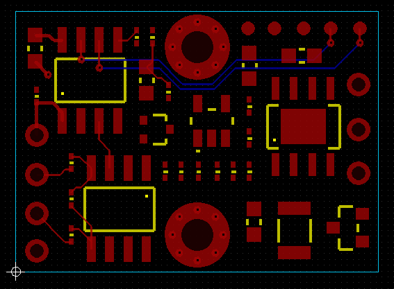
A redesign doesn’t have to be a massive undertaking, particularly if you have the original CAD data for your product. For example, a different voltage regulator probably comes in a different package, and needs a change to the PCB footprint, but that may be the full extent of the changes to your board which are needed. Build a small prototype batch, make sure they work just as before, and you’re back in business – literally.

It’s a bigger job if the part being replaced is special or complex. Changing a CPU or FPGA might be fairly straightforward in hardware terms, but require code to be recompiled, hardware drivers to be rewritten, and thorough testing to ensure everything still works as it should. A uniquely capable analogue component may have no simple replacement available, so that part of your circuit may need more extensive redesign work.

6) Call the experts

If you’re considering that a redesign might help keep production on schedule or your product’s build cost under control, give us a call.

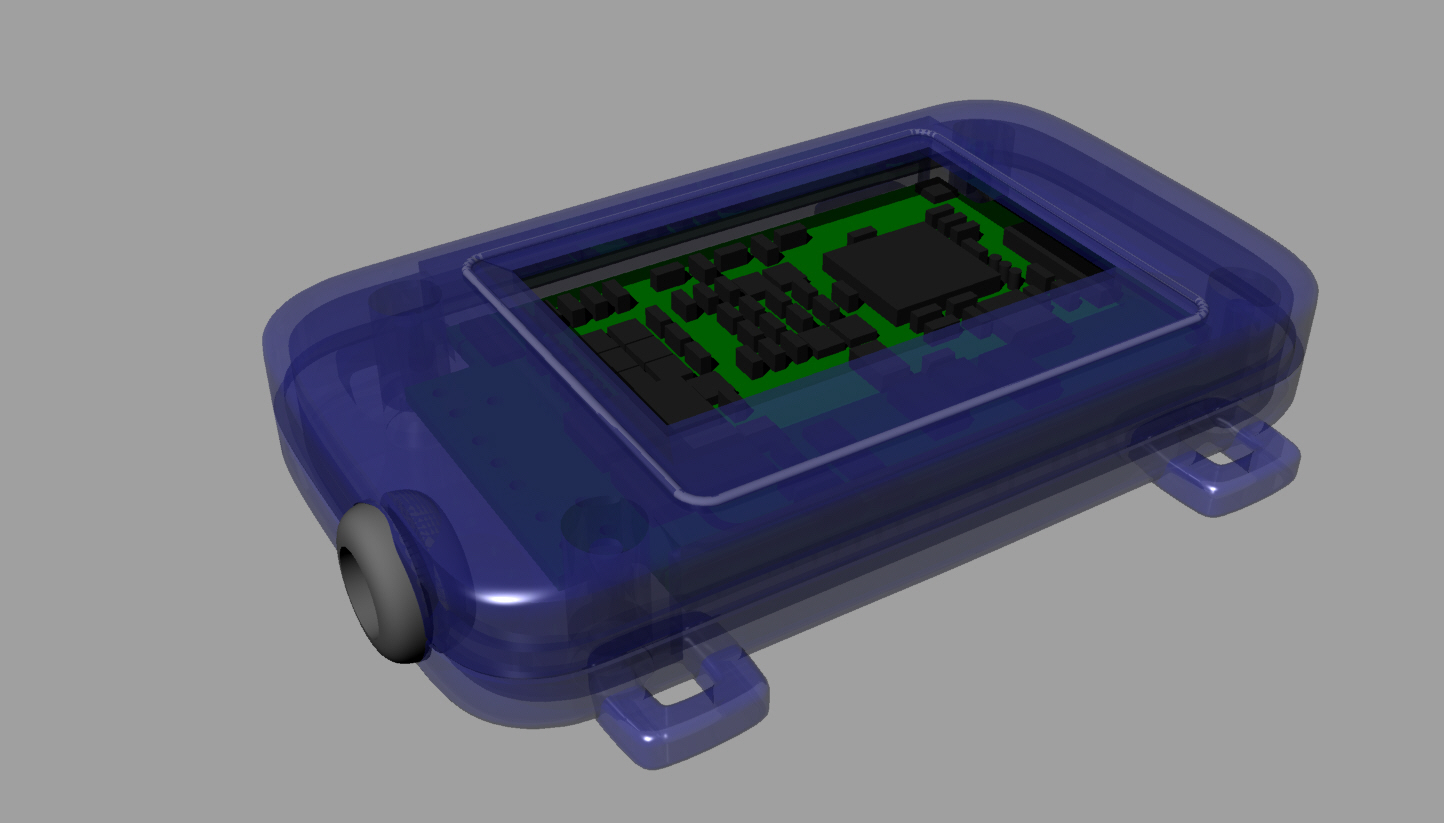
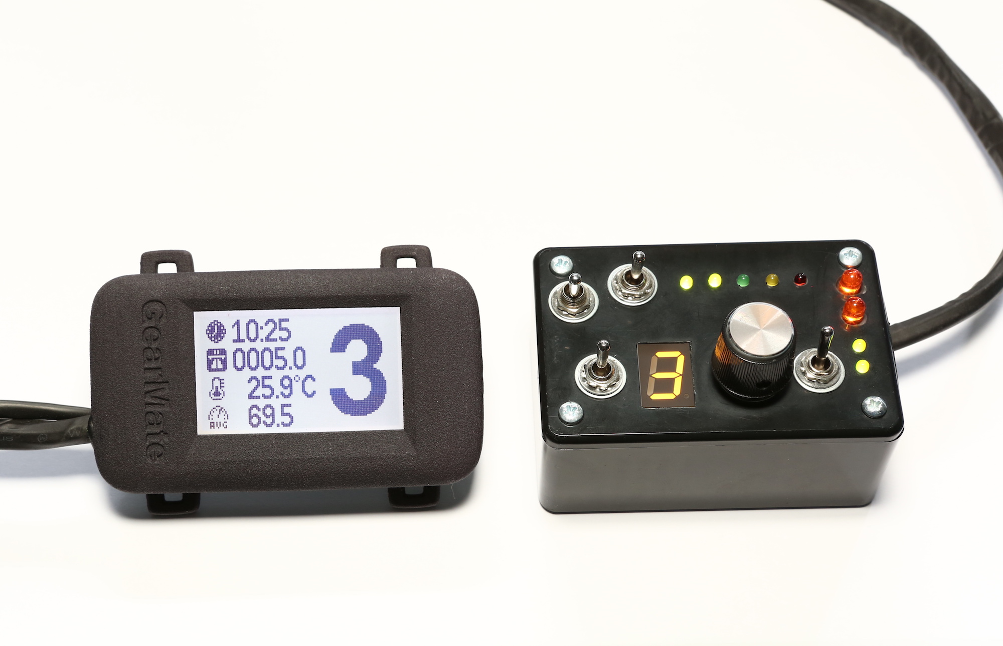
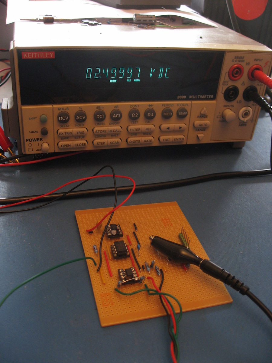
CEL has done numerous redesigns of successful products throughout 2022 for exactly these reasons. Some of these have been very simple, some much more extensive, but all have had one overriding priority: to keep production lines going despite well-known and much loved components suddenly becoming unobtainium.

Our ‘market aware’ design process is along the following lines:

  • Review the BoM and identify those components which need to be designed out.
  • Review what those components do and the circuits into which they’re incorporated.
  • Develop alternative circuits using parts which are known to be available to purchase at the time.
  • Purchase the parts for the new design in sufficient quantity to meet foreseeable production requirements.
  • When – and only when! – those parts are in the physical possession of the customer, complete the new design and prototype it.

The worst case scenario is that the newly developed board still cannot be manufactured because some component has become unobtainable during the redesign period. Stocking up on each and every line item is the best way to ensure that, regardless of what happens in the market, you’re guaranteed to be able to manufacture a reasonable number of units.

From the sale of these you can recoup the cost of components that you were able to purchase from reputable suppliers at reasonable prices. You’re protected from predatory pricing and other hazards that come with buying on the grey market.

Every new design carries risks, but it’s very unusual to design a high value component into rev ‘A’ of a board, only to design it out again in rev ‘B’.

Most changes between prototypes and production are usually to the wiring (net list), to the values of resistors and capacitors, and the addition of extra parts because it’s always fun to add a new feature at the same time. Unused parts rarely represent a lot of value tied up, and their cost shouldn’t be a major concern, especially compared to the alternative.

What shouldn’t we do?

1) Don’t panic!

The entire industry is going through a difficult time; your customers will understand, and your competitors have it just as bad as you do. We’re all in this together, and that’s unprecedented.

If your prices need to go up to cover your costs, chances are that’s as OK now as it’s ever been. If your lead times need to extend too, that’s also not going to surprise or offend anyone – but if you can keep delivering on schedule while your competitors’ deliveries slip, then you have a competitive advantage that’ll help your reputation no end.

Reviewing your designs and making changes well in advance to avoid delays or significant price hikes can help a lot here.

2) Don’t allow the quality of your product to slip

It might be tempting to waive through a board which is missing a part that’s normally needed for EMC, safety or reliability reasons. Supplies of components like filters and TVS diodes have been among the worst hit thanks to demand from the automotive sector, but they can also be some of the easiest to substitute with alternatives.

Change a footprint, maybe find a way to fit an alternative by hand, but don’t omit something that might lead to a warranty claim or worse. Don’t risk that ‘bad batch’ that harms your reputation long after the market has returned to normal.

3) Don’t buy from suppliers you wouldn’t normally buy from

Most manufacturers have had to at least consider buying components from the grey market over the last year or so. CEL normally advises customers only to ever buy from franchised distributors, but these are strange times and it helps no-one to insist on something that’s just not practical.

Buying from the grey market carries significant risks for the uninitiated, though.

Franchised distributors carry with them the reputation of the manufacturers they represent. They tend to maintain very high standards in terms of component handling and packaging, and follow the correct, necessary precautions against damage from ESD, moisture and mechanical abuse. Components are brand new, genuine, have passed factory testing, and have good shelf life. They usually sell at a fair price too, though under normal market conditions that’s something we all love to debate.

These things are not true of all grey market resellers, though.

Some are, of course, entirely legitimate, reputable organisations who trade genuine, quality product and maintain high standards throughout.

Others are not, and CEL has heard all too many horror stories this year about counterfeit parts, “factory oversupply” chips that turn out to be faulty, and suppliers who think nothing of jacking up the price and/or MOQ of an in-demand component even after an order has been accepted and paid for.

4) Don’t be held to ransom

There are suppliers who advertise good stock of parts which are otherwise hard to find, and chances are the chips simply don’t exist. Or if they do exist, the price is wildly, abusively, coffee-meets-keyboard crazy – and no, you don’t need the chips that badly.

At the very least, haggle hard, and make sure the supplier knows there’s a point at which it makes much more sense to design out their precious chips than be ripped off. Just because they’re asking “double it, then add a zero” compared to the regular price doesn’t mean you need to pay that much, or that anyone else will either.

Ultimately they need to sell the chips that they’ve paid good money for. It’s better for both parties that they sell them (even at a loss) to a genuine OEM who needs them, then not sell them at all. They may need reminding of this, even if it’s not what they want to hear.

5) Don’t go it alone

The current state of the components market is a major challenge for us all.

With over 25 years of design experience to draw upon, CEL has helped customers successfully keep their production lines going throughout 2022, and has the expertise to help you do the same – whether your electronics are a CEL design or not.

Need Help ? Contact Us

Electronics Product Design

Whether you have a detailed specification or just a bright idea, we can help you turn it into a production ready design, backed up by all the CAD data and software, plus the support you need for as long as you need it.

Fix & Improve

Do you have an existing design with a problem, or which doesn’t quite do what you need it to? CEL can help make it better.

The Process

We’re keen on communication. Let us take the time to really understand what you need, and explain how we can help.

Specialist Areas

Need something a little out of the ordinary? We may well have been there before.

Design focus: High speed digital design and termination

How are high speed digital signals terminated on a PCB?

This article explains why termination is needed in a high speed digital design, and why different types of termination are used.

What is a transmission line?

At high speeds the traces on a PCB can no longer be regarded as simple wires that cause two points on the board to always be at exactly the same potential. A PCB trace has series inductance and resistance, and distributed along its length it has capacitance to ground.

These parasitic elements are impossible to eliminate, but their values can be determined from the geometry of the trace and the stack-up of the PCB. For simulation purposes the trace can be modelled as a string of discrete inductors and capacitors; the pure dc resistance is usually negligible in high speed applications and can be ignored.

A not-at-all-obvious mathematical result is that a free end of a long PCB trace, routed on a layer above a GND plane, behaves like a resistor to GND. This behaviour persists for as long as it takes a propagating wave to travel the entire length of the trace and bounce back toward the transmitter; if the trace were infinitely long, the round trip time would also be infinitely long, and the trace would look just like a resistor to GND indefinitely.

The value of this “resistor” is called the characteristic impedance of the trace. The amount of time for which the trace looks like a resistor depends on the round-trip delay for a wave propagating along it, which in turn depends on its geometry, materials and length.

A PCB trace (or other conductor) which is long enough that this behaviour must be taken into account is referred to as a transmission line.

Why does signal integrity matter?

The input of a digital device has a maximum voltage that is guaranteed to represent a logic ‘0’, a minimum that is logic ‘1’, and a region in between through which the signal must transition monotonically if the device is to function reliably. This is of particular importance on clock inputs, where any reversal of direction within the transition region can cause the receiver to switch multiple times, resulting in data corruption.

Let’s now consider what happens when a high speed edge is generated at the output of a digital device, and switches from a logic 0 (0V) to 1 (3.3V). For the purposes of this example, the edge has a rise time of 200ps and switches at a rate of 10 MHz.

The first thing to note is that the 10 MHz switching rate is irrelevant. The phenomena which govern signal integrity on a high speed signal relate to the edge speed, not the number of edges/sec, so slowing down the clock makes absolutely no difference to whether or not a given layout will work properly.

In the first example, the PCB trace is modelled as a string of discrete L-C blocks, each consisting of 1nH in series and 1pF to GND. As a rough rule-of-thumb, 1mm of trace equates to 1nH of inductance, so this trace is not in fact particularly “long” in absolute terms. The characteristic impedance of this particular trace is about 32 Ohms, which is within the normal range for a mass produced multilayer board using conventional geometry. The transmitter is modelled as an ideal voltage source with 1 Ohm output resistance and a rise time of 200ps.

The signal at the transmitter switches cleanly from 0 to 3.3V in the expected 200ps and looks fine, but the signal at the receiver is very different. It peaks at over 6V and oscillates many times before eventually decaying away and setting at the expected logic ‘high’ level. The falling edge behaves the same way and dips below -3V before settling to GND potential. Not only does the signal contain multiple switching edges that can corrupt data and cause clocked circuits to misbehave, but the voltage swings can easily exceed the absolute maximum ratings for the receiver and damage it.

To understand why this occurs, we can look at the components in our trace model at each end of the line. When the output of the driver goes high, C1 is initially discharged and L1 sees the full logic supply voltage across it. This causes the current through L1 to ramp up, charging C1, and so L2 starts to see a voltage, and so on. The voltage wave propagates from transmitter to receiver, charging each capacitor in turn, until the wave reaches the final elements in the chain. This doesn’t happen instantaneously; it takes time, which depends on the inductance and capacitance per unit length of trace.

Since the receiver is high impedance, any current through the last inductor has nowhere to go other than the final capacitor element (which will also include the parasitic capacitance of the receiver, and possibly your scope probe if you have one connected). This current charges the capacitor, causing the voltage across it to increase.

The increase continues until the current through the final inductor reaches zero. This occurs when the voltage at the receiver Vrx equals 2x the initial height of the edge at the transmitter Vtx, and results in the wave propagating back along the trace in the opposite direction, back towards the transmitter.

This doubling of voltage and reversal in direction is characteristic behaviour of an unterminated transmission line.

Image shows Unterminated line

When the wave arrives back at the transmitter it must meet another boundary condition, namely that the voltage at the output of the transmitter is fixed, but the transmitter can sink or source current in order to maintain this state. The transmitter must now sink current in order to maintain a constant output voltage, and the result is that the wave once again reverses direction and propagates back towards the receiver.

Because neither an inductor nor a capacitor can dissipate energy, the energy has nowhere to go except to transit up and down the trace repeatedly, resulting in the rapid oscillation we see. It eventually decays away because of the 1 Ohm output resistance in series with the transmitter; without this, oscillation continues indefinitely.

Clearly this is not usable.

How does series termination improve signal quality?

Now let’s consider what happens if we put a resistor, with a value equal to the characteristic impedance of the trace, in series with it. The resistor is physically located right next to the transmitter, and adds to the internal resistance of the driver. This topology is referred to as ‘series termination’.

Image shows Series terminated line

The signal at the receiver is now clean and square – but why?

The signal at the transmitter itself is the same, but recall that the PCB trace looks like a resistor to GND until the wave has completed a full round-trip. This resistor forms a potential divider with our series terminator, resulting in an output voltage at the start of the trace which is exactly half of the logic ‘1’ level. As before, this wave propagates along the trace toward the receiver, whereupon it doubles in amplitude and reverses direction.

Now, though, rather than presenting a problem, this doubling of amplitude is exactly what’s needed to make the signal reach a valid logic ‘1’ level. The voltage at the receiver switches monotonically from logic ‘0’ to ‘1’ just as required.

The reflected wave travels back up the trace to the transmitter, but now instead of meeting an (ac) short to GND, it sees an impedance equal to the characteristic impedance of the trace. In terms of its electrical characteristics, this resistor looks to the wave just like an infinitely long extension of the transmission line, so there is no reflection; instead, the energy in the wave is dissipated as heat in the resistor, and the current in the trace falls to zero. With zero current flowing in the potential divider, no voltage is dropped, and so the voltage on both sides of the termination resistor now equals the full logic ‘1’ level and the system is stable.

This termination scheme is popular but is not without problems. A clean, monotonic edge is seen at the receiver, but not at the transmitter, nor at any other point along the length of the trace. Instead there’s a period of time for which the voltage sits at half the logic ‘1’ level, which is right in the middle of the transition region for most digital inputs, and likely to cause problems. Therefore, series termination is generally OK for point-to-point routing (one driver / one receiver), but is not suitable for cases where a single output must drive multiple inputs located in different places on the PCB. If one output must drive multiple inputs, then each input must have its own trace and series terminating resistor.

Another option is parallel termination. In this case a resistor, again equal to the characteristic impedance of the trace, is connected between trace and GND at the receiver.

There is no dividing down of the output voltage at the driver, so a wave with an amplitude equal to the full voltage swing of the driver travels along the transmission line.

When the wave arrives at the receiver it is immediately absorbed by the terminating resistor, which looks to the wave like an infinitely long extension of the trace. No reflection occurs, so the system reaches steady state after a single transit time. Every point on the trace transitions cleanly from logic ‘0’ to ‘1’ subject only to a pure propagation delay, and so high impedance receivers can be connected at any point or points along the trace.

This makes parallel termination useful for distributing clocks and other common signals to which multiple devices must be connected, but there’s an important caveat – the dc current is not zero. In this example, using 3.3V logic and a 32 Ohm trace, the driver must continually source 100mA, and the terminating resistor must dissipate 320mW of heat. Often this is not acceptable for power and thermal management reasons.

Parallel termination can also be used in multi-master interfaces, by putting a terminating resistor to GND at both ends of a long trace. Multiple drivers and receivers can be located along its length, and good signal quality is seen at every point on the trace. Terminating both ends of the transmission line does, of course, doubles the wasted current, but is still useful in applications such as long backplanes which may be driven from any one of a number of plug-in cards.

As well as being used on PCBs, parallel termination is also used in interfaces such as the automotive CAN bus.

Image shows Parallel terminated line

What other options for termination are there?

One other option, less often used, is to parallel terminate with an R-C network. A capacitor is used to block the dc current, and a resistor provides termination for ac signals as before. This can be beneficial, but has problems of its own; a real capacitor has ESL and can introduce frequency dependent issues that are hard to predict or probe.

Another option is to terminate not to GND, but to an intermediate voltage half way between the logic ‘0’ and ‘1’ levels. This reduces the wasted current by half, and for a signal which spends 50% of its time in each state, the average power wasted in the terminating resistor is also halved. One common interface which uses this mid-point termination voltage is DDR2.

Conclusions

– The need to treat a PCB trace as a transmission line, and terminate it correctly, depends on how long it is and how fast the driver switches between ‘0’ and ‘1’.
– A poorly terminated design which is experiencing errors due to signal integrity can NOT be made to work by slowing the clock down.
– Successfully designing a high speed digital system requires good knowledge of the underlying physics.

Need Help ? Contact Us

Electronics Product Design

Whether you have a detailed specification or just a bright idea, we can help you turn it into a production ready design, backed up by all the CAD data and software, plus the support you need for as long as you need it.

Fix & Improve

Do you have an existing design with a problem, or which doesn’t quite do what you need it to? CEL can help make it better.

The Process

We’re keen on communication. Let us take the time to really understand what you need, and explain how we can help.

Specialist Areas

Need something a little out of the ordinary? We may well have been there before.

Design focus: parasitic inductance | high frequency digital circuit

Design focus: parasitic inductance

Powering a high frequency digital circuit means providing a supply with an adequately low impedance across the entire frequency range from DC up to the highest frequency present in any digital switching edges. Correctly designed power distribution is crucial to achieving reliable operation and low RF emissions.

The frequency range over which a power supply must maintain low impedance is a function of the fundamental switching speed of the device used, not simply the number of edges per second. This means good high frequency decoupling is required regardless of whether the clock is running at just a few Hz, or hundreds of MHz, or somewhere in between.

Before starting a high speed PCB layout, it’s worth taking a moment to do a few rough calculations. For a trace 0.15mm (6 mils) wide in 1 oz copper, the inductance of 1mm is ~0.6nH. This will resonate with a 100nF capacitor at 20.5 MHz, and at frequencies higher than this the impedance of the supply is dominated by this inductor, not the capacitor.

All this happens at frequencies which are much lower than the frequencies contained within digital switching edges, which is why great care must be taken in the placement and routing of decoupling caps in digital circuits. The parasitic effect of a short PCB trace may completely negate the benefit of a decoupling capacitor in a given location.

Conversely, it may also be possible to minimise the number of decoupling caps that are required in a given design by improving the layout.

– Remember that it is inductance, not resistance, that dominates the impedance between two points on the PCB.

– The lowest inductance route between any two points is through a solid, uninterrupted plane – even if this means the path length between them is greater than it would be if they were joined by a thinner trace on the same layer. The shortest physical distance may not correspond to the shortest electrical distance.

– The parasitic inductance of a ceramic capacitor depends on its physical size. For two capacitors of equal case size (eg. 0402) but different values, the one with the higher value will have a lower impedance at most frequencies than the one with the lower value, making it the better choice for decoupling.

– A single capacitor joined into its power plane with two traces and vias at each end may be just as effective as two separate capacitors routed with one trace and via each. That same capacitor connected using planes on the component side of the PCB, and stitched into the buried power and ground planes using multiple vias, will be more effective still.

A SPICE simulation clearly shows the difference:

– the green trace represents the impedance of C1, value 100n, with 1mm of trace attached. Resonance occurs at 20.5 MHz as expected, above which the inductance becomes dominant.

– the blue trace represents C2, which is 10n but otherwise identical. Although resonance occurs at a higher frequency (65M), the absolute impedance of C1 (and its ESL) is still significantly lower all the way up to 48M, and there’s negligible difference from 100M upwards where both become dominated by their ESL.

– the red trace shows a single 100n capacitor but connected by two traces in parallel rather than just one. Its impedance is lower than either of the other two across the entire frequency range apart from a very narrow window where the 10n cap resonates. In particular, it maintains a significantly lower impedance at high frequencies.

Simple changes to a board layout can improve its high frequency performance enormously, and a clear understanding of how the layout will affect the performance of the design is crucial to producing boards which are reliable and which can pass EMC testing.

Do you have a new digital design project in mind?

Or a board which is failing emissions testing?

CEL has years of experience in high speed board design and layout, signal integrity and EMC.

Contact us today to see how we can help.

CEL lab tour: power supplies

CEL lab tour: power supplies

A bench power supply is at the heart of every electronics workstation. A modern switched-mode supply is compact and efficient – so why does CEL use these older units that are big, heavy, and which keep the lab warm in winter?

The HP / Agilent 663xB series is a linear design, which means the output is ultra clean with no switching noise that can interfere with the connected equipment.

One of CEL’s specialist areas of expertise is in ultrasonics, where the signals received from transducers are very small, and the precision with which they can be measured determines the accuracy of the finished product. Having a source of power which is free of RF noise is essential when developing these sensitive circuits – even if the finished product won’t have this luxury.

The 663xB series is also able to sink current as well as source it, which means it can be used to simulate a rechargeable battery. With mutiple PSUs, one can substitute for the project’s battery (in any chosen state of charge) while others supply the charging current and whatever voltage rails the project requires for its own use. Each PSU also includes accurate current and voltage meters, removing the need for separate multimeters and ensuring no unexpected conditions go unnoticed.

Recent projects for which the particular capabilities of the 663xB were useful have included:

– functional testing of power supplies which were customer returns, to determine whether or not they were genuinely defective, and if so, the root cause of the failure and the possible consequences for the equipment they were powering

– developing an automotive project which contained its own Li-ion backup battery, designed to maintain power to the equipment when disconnected from the vehicle supply

– determining the true resistance of automotive power cables, which were suspected of not meeting their published specifications for conductivity and copper content

CEL has all three models in the 663xB series: the 6632B (20V/5A), 6633B (50V/2A) and 6634B (100V/1A), so all requirements from low voltage logic up to 24V automotive supplies and beyond are covered.

3D printing at CEL

Every electronic device is a part of a larger assembly. Whether it’s just a box to house a PCB, or a complex assembly with moving parts and sensors, 3D printing is the modern way to produce high quality, functional prototypes.

CEL’s printer is an SLA machine, which uses ultraviolet light to expose a UV sensitive resin one layer at a time in order to build up a complete 3D object.

The UV light is shone upwards into a tank of resin through its transparent base, using an LCD shutter to ensure only those areas which should become solid are illuminated. After each layer has been exposed and solidified, the model is raised up slightly and the process repeats until the entire object has been drawn up out of the tank.

Each layer can be as thin as 25 microns, which means the level of detail and quality of surface finish are excellent. Models are strong, dimensionally accurate, and have few limitations in terms of the shapes and geometries that can be produced. Resins come in a range of colours including transparent, as seen here.

Contact CEL to see how 3D printing could get your next project to market sooner.

CEL Design Example
Motorcycle Gear Indicator

Not everything which CEL designs is made for mass production. We also make one-offs, demonstrators, in-house test equipment and other projects which are only ever intended to be made in small numbers.

The device on the left was produced by CEL as a demonstration of how an auxiliary display and accessory controller for a motorcycle might look and operate. It’s wired into the bike’s existing wiring harness and displays various useful pieces of information such as which gear the bike is in, average speed, air temperature and estimated fuel range remaining.

Its internal processor derives this information by timing and counting pulses which indicate road speed and engine rpm. A learning feature allows it to adapt automatically to the signals produced by numerous different makes and models of bike, meaning it would be suitable to build and sell as an aftermarket accessory without the need to stock multiple different variants.

Particular emphasis was placed on ease of set-up by the end user, the process requiring nothing more technical than riding the bike in each gear for a few seconds, so the device can analyse the signals from the bike and learn its gear ratios.

Several units were hand assembled into 3D printed enclosures, and even though it was never intended to be made in quantity in that form, features from it were incorporated into other products which you can buy from a high street automotive parts store today.

On the right is a true one-off – a battery powered motorcycle simulator, which provides power and produces signals (eg. for road speed and engine rpm) equivalent to those available on a real bike. It has controls to replicate ignition, clutch and gears, allowing all the features of its companion device to be demonstrated in a way which is portable and convenient.

Wolf Elec Ltd
Vehicle Intercoms

CEL was approached by Wolf Elec Ltd, a manufacturer of intercoms, security systems and other accessories for specialist and commercial vehicles.

Wolf Elec were looking to supply a voice intercom system as an OEM component for a new purpose built taxicab. A key requirement was that, in addition to driving loudspeakers, new regulations demanded that the intercom support an induction loop for use by passengers who use hearing aids.

CEL developed a novel amplifier which was able to provide clear audio over the entire frequency range, with no more adjustment required than a simple volume control, even when the induction loop was installed in close proximity to the metal roof of the vehicle. Nearby metal normally tends to reduce the signal strength and muffle higher frequencies, which would make the driver of the taxi harder to hear clearly.

Working alongside the customer’s existing design and manufacturing partners, CEL produced a final circuit which was then tuned in the vehicle itself to optimise audio quality. Software algorithms and audio levels were adjusted to give the driver, hearing passengers and hard-of-hearing passengers a clear, unobtrusive experience.

The design also incorporated software features which allowed it to replace several different older intercom PCBs in other applications, including ones on which components had gone end-of-life and were becoming increasingly hard to obtain.

The finished product is now in mass production, and next time you ride in a taxi, you may well find yourself using it without even knowing!

Reventec Ltd
Torque Sensor

CEL was contacted by Reventec Ltd, a manufacturer of sensors which are used by the professional motor racing industry, as well as in other applications which demand high reliability at elevated temperatures and under severe vibration.

Reventec was looking to produce a strain gauge with a 0 to 5V output for measuring the torque applied to the steering column of a racing car. Previously they had been buying in an amplifier from a third party, but it was quite expensive, too large, and required adjustment using a screwdriver which meant it could not be fully encapsulated to protect it from vibration.

CEL designed a prototype circuit around the Analog Devices AD8557 digitally programmable amplifier IC. This device can be programmed to adjust its gain and offset without the need for a physical potentiometer. To control this device and allow it to be adjusted easily, CEL developed software for a Microchip PIC which presented a simple command line interface that could be used via terminal software on any laptop.

The CEL software included a self-calibration facility, so the previously time consuming and fiddly process of adjusting out the zero offset was replaced by a single command taking just moments to execute.

The hardware was first prototyped on stripboard, allowing it to be debugged and demonstrated before committing to a PCB. Finally the board was laid out and sent off for manufacture, with the final design being just 18x25mm.

As well as all the CAD data and source code, Reventec was provided with full documentation describing how the board works, how to connect it up, and how to adjust the gain and offset for any given application using the serial interface.

In this case a clear understanding of the needs of the application resulted in a simple, inexpensive PCB which was quicker to assemble into a finished sensor than an off-the-shelf board, as well as being more robust, accurate and versatile.

Firestone Technology Ltd
Wireless Thermostat

Firestone manufactures Dragon Bench, a heated outdoor seat intended as an energy-efficient replacement for patio heaters outside bars and restaurants.

CEL had already designed a simple thermostat to regulate the temperature of these heated bench seats, and so was the natural choice when Firestone wanted to upgrade the system to permit centralised monitoring and control of multiple units from a single location. Their requirement was to have a device behind the bar which would be able to set and show the temperatures of all the heaters, turn them on in time for dinner service and off at the closing time, and indicate any faults that required attention.

Working together with software engineers at Firestone, CEL developed a smart thermostat around a Zigbee wireless network. The Zigbee standard was chosen because it forms a ‘mesh’ network, in which any device can communicate with any other by automatically routing traffic via intermediate devices. This would mean that benches could be spread over a large commercial outdoor space with no need to have all of them within the radio range of the bar.

With an eye on ensuring the system remained trouble-free and reliable, features were included to secure it from unwanted radio interference, whether benign, malicious or just a nearby neighbour with the same kit.

For simpler installations with only a few benches, the CEL thermostat also included an LCD display, buttons and a real-time clock, so it could be programmed to switch on and off at different times according to a weekly schedule. The option was provided to omit the wireless module on these units to save manufacturing cost.

The finished product was a true collaboration between Firestone and CEL, with CEL providing electrical design, specifications and firmware, and Firestone taking care of the mechanical design, the central controller and the heated benches themselves.